
Author Affiliations
Abstract
1 National Key Laboratory of Materials for Integrated Circuits, Shanghai Institute of Microsystem and Information Technology, Chinese Academy of Sciences (SIMIT, CAS), Shanghai 200050, China
2 State Key Laboratory of Dynamic Measurement Technology, School of Instrument and Electronics, North University of China, Taiyuan 030051, China
3 Center of Materials Science and Optoelectronics Engineering, University of Chinese Academy of Sciences, Beijing 100049, China
4 e-mail: xiaoyou@mail.sim.ac.cn
5 e-mail: lihao@mail.sim.ac.cn
6 e-mail: wuaimin@mail.sim.ac.cn
Superconducting nanowires enable the operation of outstanding single-photon detectors, which are required particularly for quantum information and weak-light measurement applications. However, the trade-off between detection speed and efficiency, which is related to the filling factors of superconducting nanowires, is still a challenge. Here, we propose a fast, efficient single-photon detector fabricated by integrating ultralow-filling-factor meandered superconducting nanowires atop a photonic crystal (PhC) resonator. This unique structure enables a fast photon response due to the low kinetic inductance of the short nanowires and ensures efficient photon absorption due to the resonant effect of the PhC structure. The proposed detector has a filling factor of only while maintaining a high maximum absorption in our simulation of 90%. The fabricated device exhibits a maximum system detection efficiency of 60%, a maximum count rate of , and a recovery time of only , which is three times faster than that of the conventional meandered structure at the same sensing diameter (18 μm). This work helps advance the movement toward high-efficiency, high-speed single-photon detectors and promotes their future application in quantum communication and imaging.
Photonics Research
2023, 11(12): 2128
大连理工大学材料科学与工程学院 辽宁省能源材料及器件重点实验室, 辽宁 大连 116024
随着消费类电子、电动汽车和储能等领域的迅猛发展, 亟需提升以锂离子电池为代表的二次储能设备的能量密度, 而正极材料是提升锂离子电池能量密度的关键。富锂锰基层状氧化物正极材料(LRM)因具有极高的理论比容量(>350 mA·h·g-1)和可逆比容量(>250 mA·h·g-1)被认为是最有前途的锂离子电池正极材料之一。然而, LRM正极材料的首次Coulombic效率低、倍率/性能差以及快速的电压和容量衰减等问题, 严重阻碍了其产业化应用。本文介绍了LRM正极材料的晶体结构及电化学机理等方面的研究进展, 分析了LRM存在的问题及起因。重点从形貌设计调控、掺杂、包覆、缺陷结构设计、梯度成分设计、层状/尖晶石异质结构构建以及电解液添加剂等方面全面介绍了LRM正极材料的改性策略, 以期望为LRM正极的未来发展提供思路和指导, 最终促进LRM正极材料的实际应用。
锂离子电池 富锂锰基正极材料 晶体结构 反应机理 改性策略 lithium ion battery lithium-rich manganese-based cathode materials crystal structure reaction mechanism modification strategy

Author Affiliations
Abstract
1 State Key Laboratory of Functional Materials for Informatics, Shanghai Institute of Microsystem and Information Technology, Chinese Academy of Sciences, Shanghai 200050, China
2 Center of Materials Science and Optoelectronics Engineering, University of Chinese Academy of Sciences, Beijing 100049, China
3 Key Laboratory of Terahertz Solid State Technology, Shanghai Institute of Microsystem and Information Technology, Chinese Academy of Sciences, Shanghai 200050, China
4 Centre for Optical and Electromagnetic Research and International Research Center for Advanced Photonics, College of Optical Science and Engineering, Zhejiang University, Hangzhou 310058, China
5 e-mail: jinyi_2008@zju.edu.cn
6 e-mail: qgong@mail.sim.ac.cn
7 e-mail: wuaimin@mail.sim.ac.cn
Bound states in the continuum (BICs) can make subwavelength dielectric resonators sustain low radiation leakage, paving a new way to minimize the device size, enhance photoluminescence, and even realize lasing. Here, we present a quasi-BIC-supporting GaAs nanodisk with embedded InAs quantum dots as a compact bright on-chip light source, which is realized by heterogeneous integration, avoiding complex multilayered construction and subsequent mismatch and defects. The emitters are grown inside the nanodisk to match the mode field distribution to form strong light–matter interaction. One fabricated sample demonstrates a photoluminescence peak sustaining a quality factor up to 68 enhanced by the quasi-BIC, and the emitting effect can be further promoted by improving the epilayer quality and optimizing the layer-transferring process in the fabrication. This work provides a promising solution to building an ultracompact optical source to be integrated on a silicon photonic chip for high-density integration.
Photonics Research
2022, 10(8): 1971
1 中国科学院 上海微系统与信息技术研究所 信息功能材料国家重点实验室, 上海 200050
2 中国科学院大学, 北京100049
刻蚀衍射光栅(EDG)作为实现波分复用功能的关键器件, 对于片上光互连的实现至关重要。为了实现1310nm波段通道间隔为20nm的硅基EDG, 采用了基尔霍夫标量衍射理论仿真方法进行理论设计和仿真验证, 通过在闪耀光栅反射面引入布喇格反射光栅来提高反射效率、降低器件插入损耗, 并在入射波导处引入多模干涉耦合器以实现通道频谱平坦化设计。结果表明, 闪耀光栅反射面的反射效率由35%提高到了85%, 1dB带宽达到12nm。这对于提高系统稳定性、增大传输距离和容量、降低系统成本具有显著作用, 能够满足光互连系统的实际应用需求。
集成光学 刻蚀衍射光栅 硅基光互连 波分复用技术 integrated optics etching diffraction grating silicon-based optical interconnection wavelength division multiplex
Author Affiliations
Abstract
1 State Key Laboratory of Functional Materials for Informatics, Shanghai Institute of Microsystem and Information Technology, Shanghai 200050, China
2 Nantong Opto-Electronics Engineering Center Chinese Academy of Science, Nantong 226000, China
3 University of Chinese Academy of Science, Beijing 100049, China
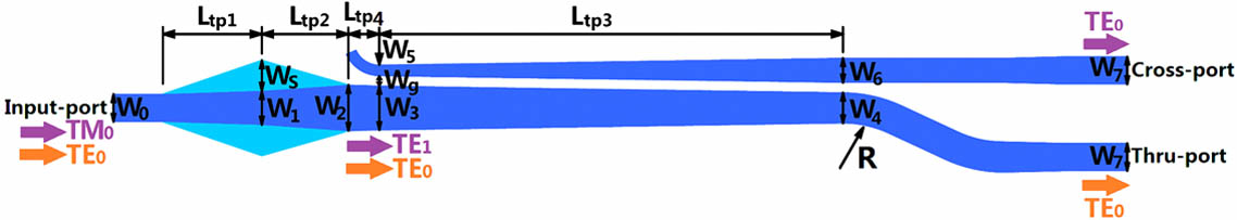
An ultra-broadband and fabrication-tolerant silicon polarization rotator splitter is proposed in this Letter. Benefitting from the broadband and low-loss characteristics of the bi-level taper and counter-tapered coupler, the designed device has a simulated insertion loss and crosstalk of less than 0.2 and 15 dB in the waveband from 1290 to 1610 nm. These characteristics make it valuable in applications with large bandwidth requirements, such as full-grid Coarse wavelength division multiplexer (CWDM) and diplexer/triplexer fiber-to-the-home systems. The fabrication tolerance of the design is also analyzed, showing that the device performance is quite stable with normal manufacturing errors in silicon photonics foundries.
130.3120 Integrated optics devices 130.5440 Polarization-selective devices Chinese Optics Letters
2016, 14(8): 081301
1 广东省微纳光子功能材料与器件重点实验室, 广东 广州 510006
2 上海市激光技术研究所, 上海 200233
3 上海市激光束精细加工重点实验室, 上海 200233
在已有实验的基础上, 利用已得实验数据, 运用逐步回归模型和B.P神经网络模型, 通过MATLAB平台进行理论计算。研究结果表明, 理论计算与实验值具有良好的吻合性, 其相对误差在8%以下, 均方根误差在0.05以内; 模型研究表明氧元素是促进铝合金焊接热裂纹增长的主要元素之一, 镁等元素则抑制热裂纹的形成; 通过采用改进的B.P神经网络模型, 对多元逐步回归模型的预测能力进行了验证, 其数值试验结果表明, 热裂纹敏感系数同各元素含量呈现拟线性的多元函数关系。该逐步回归模型能够对激光焊接铝合金热裂纹的形成进行预测及控制, 为激光焊接裂纹预测和控制的工程化应用提供一种比较可行的方法。
激光焊接 热裂纹 逐步回归 B.P神经网络 laser welding hot-crack matlab matlab stepwise regression B.P. nerual network
Author Affiliations
Abstract
A compact bi-directional (BiDi) triplexer using grating-assisted multimode interference (MMI) coupler is proposed based on silicon nanowire waveguides.Because of the high index contrast between silicon and silicon dioxide, the size of the structure is greatly reduced with a footprint of 2.5 \times 911 (\mu m). Asymmetrical ports are introduced in the MMI structure to satisfy the bandwidth requirements of the industrial standards ITU-T G.983.3-dB bandwidths of 100, 22, and 15 nm are obtained for the wavelengths of 1 310, 1 490, and 1 550 nm, respectively. The device can be readily fabricated using a commercial CMOS process.
130.3120 Integrated optics devices 230.7390 Waveguides, planar 060.4230 Multiplexing Chinese Optics Letters
2013, 11(4): 041301


